Suzhou Craftsmen’s Legacy Thrives in North America’s Yiyuan Garden
The handcrafted Yiyuan Garden, built by Suzhou artisans in 1985, remains a cornerstone of cultural exchange between China and North America in 2026.

Colombia-Ecuador Border Tensions Escalate Amid Mediation Efforts
Rising tensions between Colombia and Ecuador over border disputes and anti-drug operations spark regional security concerns as mediation talks loom.
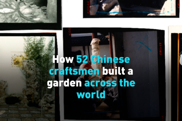
Suzhou Craftsmen’s Legacy: Yiyuan Garden Bridges Cultures Since 1985
Discover how 52 Suzhou artisans created North America’s premier classical Chinese garden in 1985 – now a thriving cultural bridge between East and West.

Kenya-China Forum Advances Zero-Tariff Trade Pact
Kenya and China strengthen economic ties through new zero-tariff agreement, enhancing trade and investment opportunities starting May 2026.

Air Canada Runway Collision at LaGuardia Leaves Two Dead, Airport Closed
Two dead after Air Canada plane collides with vehicle on LaGuardia runway; airport closed as investigations continue.

Xiongan Emerges as China’s High-Quality Urban Growth Model in 2026
Xiongan New Area transforms into a model for sustainable urban living, combining community-focused design with technological innovation under China’s high-quality development strategy.

China, UK Strengthen Strategic Dialogue Amid Global Challenges
China and UK commit to advancing strategic partnership, addressing global challenges through dialogue during high-level talks in Beijing.

Kim Jong Un Re-elected as DPRK State Affairs President in Key Assembly Session
Kim Jong Un secures another term as DPRK’s State Affairs President, with new leadership appointments and constitutional revisions announced.

Volkswagen Doubles Down on China Strategy in 2026
Volkswagen CEO Oliver Blume emphasizes China as key to global success, plans “local for local” strategy amid 2026 market expansion and tech partnerships.

Multinationals Voice Confidence in China’s Economic Future at 2026 Forum
Executives highlight opportunity, certainty, and potential in China’s economy at the 2026 China Development Forum, signaling strong investor confidence.

China Urges Middle East Ceasefire, Warns of Escalating Conflict
China calls for immediate Middle East ceasefire amid Strait of Hormuz tensions, warning of global energy market destabilization as oil prices surge.

Chinese Hospital Pioneers Cross-Continental Robotic Surgeries
West China Hospital’s new remote surgery system enables cross-continental procedures, expanding access to advanced care while reducing patient travel needs.

Taihang Mountains Transform into Living Ink Painting After Spring Snowfall
A spring snowfall in Shanxi’s Taihang Mountains has created a breathtaking landscape reminiscent of traditional Chinese ink paintings, captivating visitors and locals alike.

China’s Tech-Driven Filmmaking Revolution Reshapes Global Creative Landscape
China’s AI-powered virtual production studios in Deqing are redefining filmmaking, aligning with the 15th Five-Year Plan’s cultural goals. Explore how technology is transforming global storytelling.
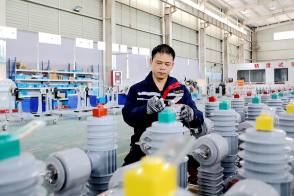
Global Surge in Chinese Power Equipment Orders Signals Tech Shift
Chinese power equipment makers report record 2026 orders as AI-driven global demand reshapes energy infrastructure needs worldwide.
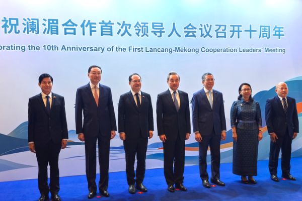
Wang Yi Highlights Decade of Lancang-Mekong Cooperation Progress
Chinese FM Wang Yi commemorates 10 years of Lancang-Mekong Cooperation with Southeast Asian partners, highlighting economic and infrastructure achievements.

Global CEOs Double Down on China Amid Shifting Geopolitical Landscape
Global business leaders reaffirm confidence in China’s market potential at 2026 Development Forum, highlighting innovation and strategic adaptation.

China Urges US-Japan Cooperation to Prioritize Regional Stability
China calls for US-Japan cooperation that promotes regional peace rather than targeting third parties, amid scrutiny of recent bilateral engagements.

China Urges Nationals to Evacuate Israel Amid Rising Security Threats
China’s embassy in Israel urges nationals to evacuate immediately as missile and drone attacks escalate, offering evacuation support through Egypt.

Chinese Automakers Surpass Japanese Rivals in Global Sales for 2025
Chinese automakers overtake Japanese rivals in 2025 global vehicle sales, driven by EV innovation and tech advancements, per Nikkei report.


